Our lives are far better today owing to that little microchip that is in every electronic device around us. Just look at our smartphone, a device that fits in our pocket, holds billions of microscopic electronic switches, executing trillions of calculations every second to process sound, video, and artificial intelligence. All of this, thanks to the advancements in the chip industry.
But, less than 100 years ago, computers far inferior to our smartphones, filled an entire room, weighed hundreds of pounds, radiated immense heat, and frequently broke down because a tiny glass lightbulb burned out.
Just 50 years ago, the microchips in computers had about 5000 transistors – tiny little electronic switches that do all the work. Latest Apple M6 processor for Mac Mini has 46 billion of them.
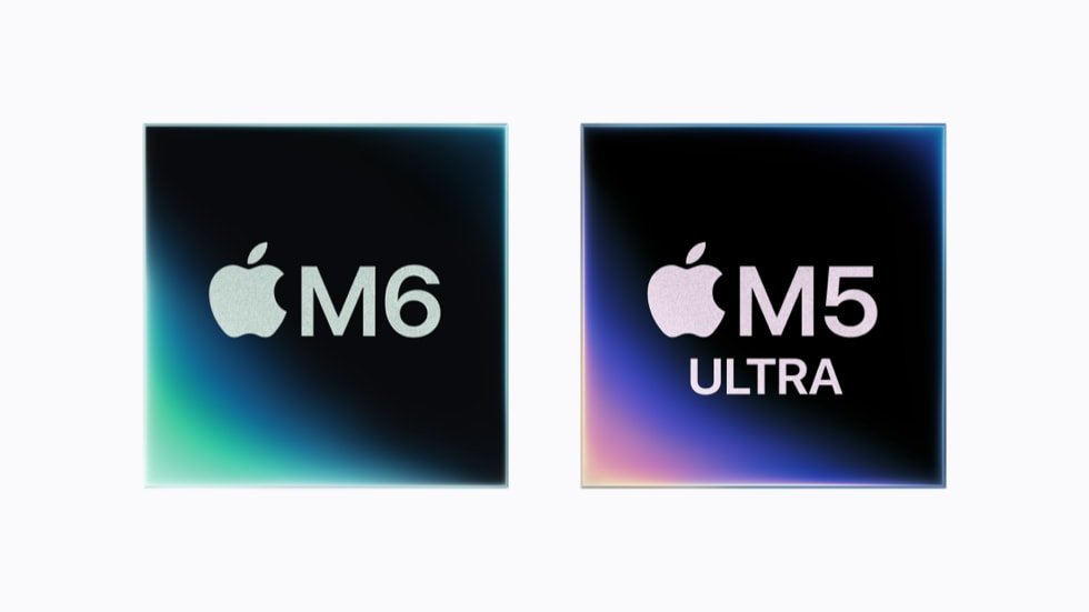
In the space taken by a single letter in this sentence, about 5-6bn transistors from M6 processor can be packed.
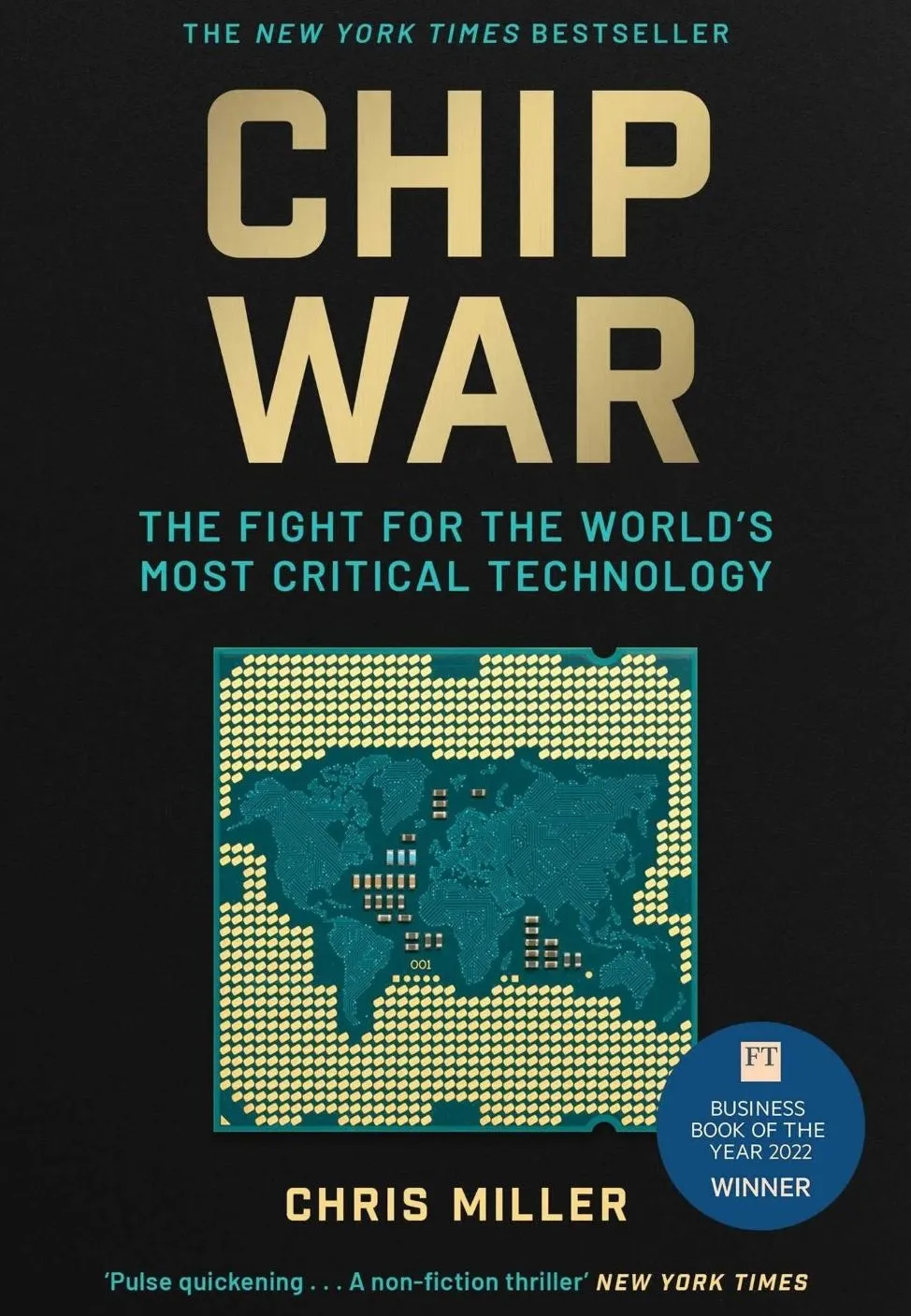
This breath-taking transformation represents the most dramatic acceleration of manufacturing precision and design capability in human history. The book Chip War: The Fight for the World’s Most Critical Technology, details how scientists and engineers pushed past the limits of physics to miniaturize computer components.
This blog post picks five breathtaking technological milestones from that book, that took us from clunky glass bulbs to sub-microscopic 3D transistors.
1. The Solid-State Revolution: Replacing Fragile Vacuum Tubes with Doped Silicon
In the early days of computing, machines like ENIAC relied on vacuum tubes—glass bulbs containing metal filaments through which electric currents flowed. By switching currents on (1) or off (0), these tubes allowed early digital computers to run binary calculations. However, vacuum tubes were notoriously slow, bulky, and unreliable, requiring complex jungles of hand-wired connections.
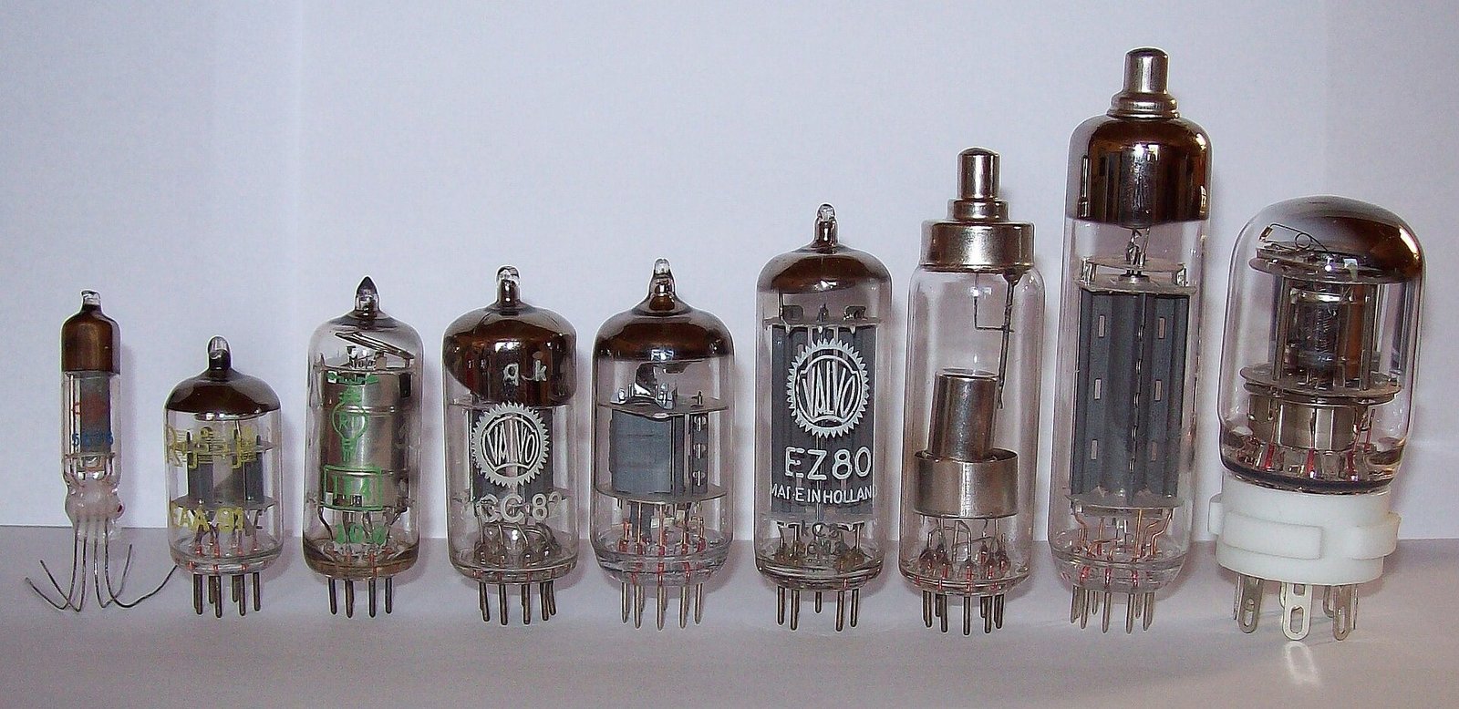
The foundational shift occurred at Bell Labs, where physicists William Shockley, John Bardeen, and Walter Brattain theorized a “solid-state valve”. By “doping” pure semiconductor materials like silicon with tiny amounts of elements such as phosphorus, researchers found they could alter the material’s electrical properties. Applying a small electric current to a middle layer of semiconductor material could turn a larger current on and off across the device, creating a solid-state switch without any moving parts or fragile glass filaments.
Why this matters: Moving from glass vacuum tubes to solid-state silicon switches eliminated mechanical fragility and massive heat generation, creating a tiny, durable building block that could be miniaturized indefinitely.
2. Photolithography: Turning Semiconductor Fabrication into “Printing with Light”
Even after individual transistors replaced vacuum tubes, engineers faced a daunting bottleneck: wiring thousands of individual transistors together by hand created a chaotic “jungle of complexity”. The breakthrough came in 1958–1959 when Jack Kilby of Texas Instruments and Robert Noyce of Fairchild Semiconductor invented the integrated circuit (chip), building multiple electronic components onto a single slab of semiconductor material.
To mass-produce these integrated circuits, engineer Jay Lathrop conceived a radical idea: turning a microscope upside down to project light through lenses and stencil-like masks onto silicon wafers coated in light-sensitive photoresist chemicals. Where light struck the photoresist, the chemical structure was altered, allowing microscopic patterns and “wires” to be etched precisely into the silicon. Lathrop named this process photolithography—printing with light.
“light rays and photoresists could solve the mass-production problem, mechanizing and miniaturizing chipmaking in a way that soldering wires together by hand could not.”
Why this matters: Photolithography transformed semiconductor manufacturing from an artisan craft of hand-soldering individual wires into an automated, high-precision printing press. This mechanized approach made mass production possible and established the scaling engine behind Moore’s Law.
3. The Shift to 3D Transistors: FinFETs and Gate-All-Around Architectures
In 1965, Fairchild’s Gordon Moore famously predicted that the number of transistors packed onto a single chip would double every year (later updated to roughly every two years). For decades, chipmakers sustained Moore’s Law by shrinking flat, two-dimensional transistors on silicon wafers.
However, as transistor features shrank toward atomic scales, physics struck back. Flat 2D transistors began suffering from severe electricity leakage—electrons bled across thin semiconductor channels even when the switch was supposed to be “off”. To overcome this wall, engineers developed FinFETs, setting the semiconductor channel on top of a block so that it protruded like a fin on a whale’s back. This allowed electric fields to control the current from three sides instead of just the top. As transistors shrink further, fin structures are being replaced by wire-shaped “gate-all-around” tubes, where the gate surrounds the semiconductor wire on all four sides.
Why this matters: When 2D physical designs ran out of steam, engineers literally built into the third dimension. Wrapping gates completely around nanoscale channels and stacking wires vertically promises up to a 50-fold increase in transistor density, proving that human ingenuity can circumvent quantum-level leakage problems.
4. Electronic Design Automation: The “Gutenberg Moment” for Chip Design
As chip complexity expanded from thousands of transistors to millions and billions, it became humanly impossible for engineers to draw every circuit path and transistor layout by hand.
In the late 1970s, Lynn Conway and Carver Mead introduced mathematical “design rules” and standard libraries of interchangeable electronic parts. This enabled the creation of Electronic Design Automation (EDA) software from firms like Synopsys and Cadence. Instead of sketching physical transistors, designers could write code and use software tools to automatically route billions of connections. Students could design custom chips on software and mail the file to a manufacturing facility without ever stepping foot inside a physical factory.
“Mead liked to think of himself as Johannes Gutenberg, whose mechanization of book production had let writers focus on writing and printers on printing.”
Why this matters: Just as photolithography mechanized physical fabrication, EDA software digitized and automated chip design. Decoupling chip design from factory management democratized chip creation, enabling software-driven startups to innovate rapidly without owning expensive manufacturing plants.
5. Extreme Ultraviolet (EUV) Lithography: Blast Waves, Plasma, and Nanometer Precision
Modern transistors are now far smaller than a human cell or even a virus particle. Because standard wavelengths of visible and deep ultraviolet light are too wide to etch features at such microscopic scales, the chip industry required an entirely new lithographic light source.
The solution was Extreme Ultraviolet (EUV) lithography, spearheaded commercially by Dutch firm ASML. EUV machines shoot lasers at falling droplets of molten tin to generate plasma that emits invisible light with a wavelength of just 13.5 nanometers. This light is focused through ultra-precise mirrors inside a vacuum chamber to carve features measured in nanometers onto silicon wafers. Each EUV system costs over $100 million and requires hundreds of thousands of hyper-specialized components from around the world.
“The miracle isn’t simply that EUV lithography works, but that it does so reliably enough to produce chips cost- effectively.”
Why this matters: EUV lithography represents the absolute pinnacle of modern industrial engineering. It proves that continuing Moore’s Law required not just better incremental designs, but orchestrating global breakthroughs in optics, laser physics, and chemistry to manipulate light at atomic scales.
Looking Ahead: What Lies Beyond the Atomic Limit?
The evolution of the transistor is a testament to human relentless operational execution and scientific intuition. We have journeyed from fragile glass bulbs to sub-microscopic 3D wire structures printed with plasma-generated EUV light, producing more transistors in recent years than all other manufactured goods in human history combined.
As we move toward specialized AI processors, vertical chiplet stacking, and gate-all-around architectures, we face new physical boundaries.
When the features on a microchip are approaching the width of individual atoms, what wild technological breakthrough do you think will carry computation through the next fifty years?